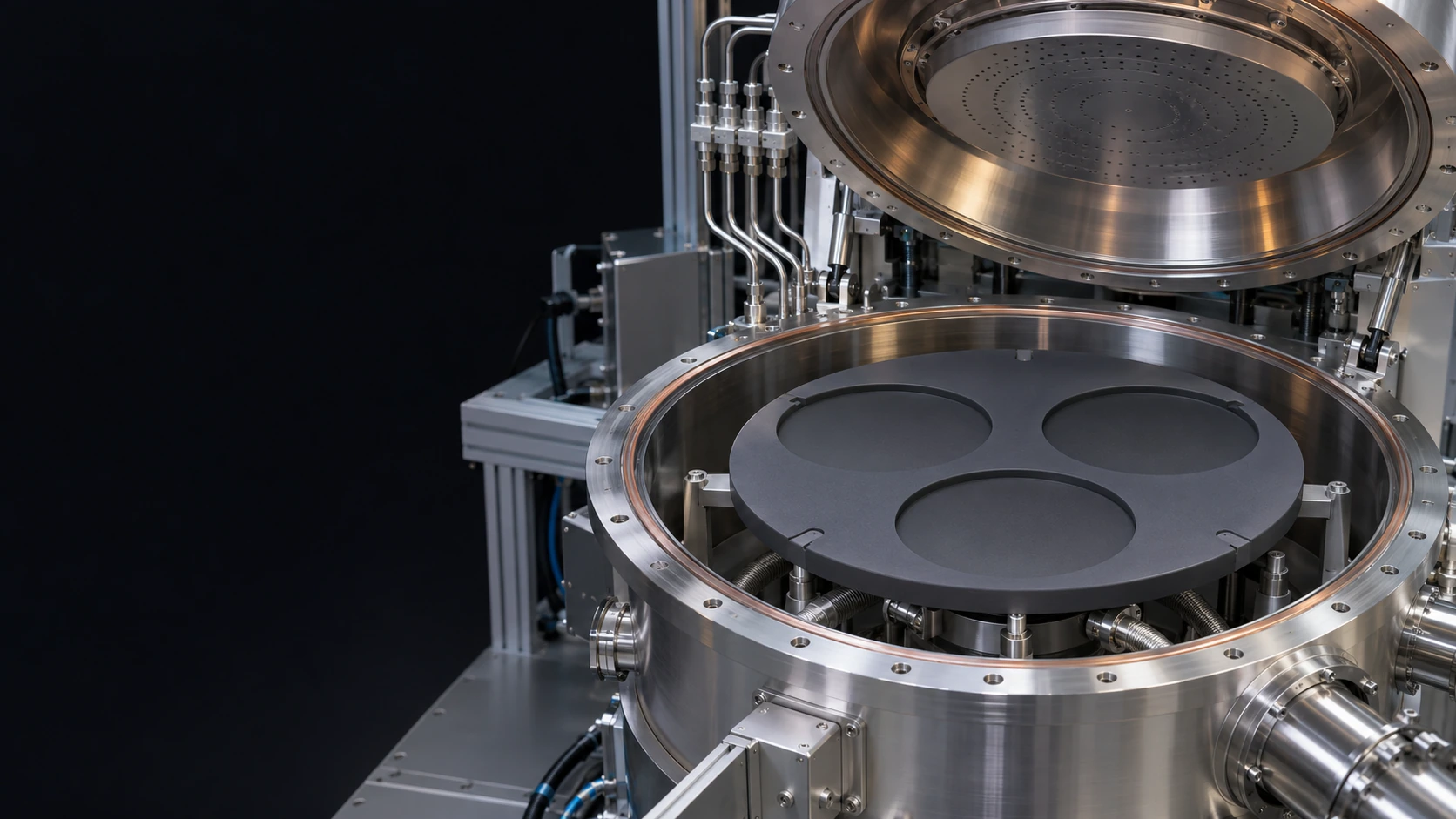
PRECISION PARTS.
PROCESS READY.
Specify coated carriers and ceramic components to fit your semiconductor process chamber.
Get a QuoteOUR PRODUCTS.
Coatings, ceramics and high-purity materials for critical semiconductor process parts.
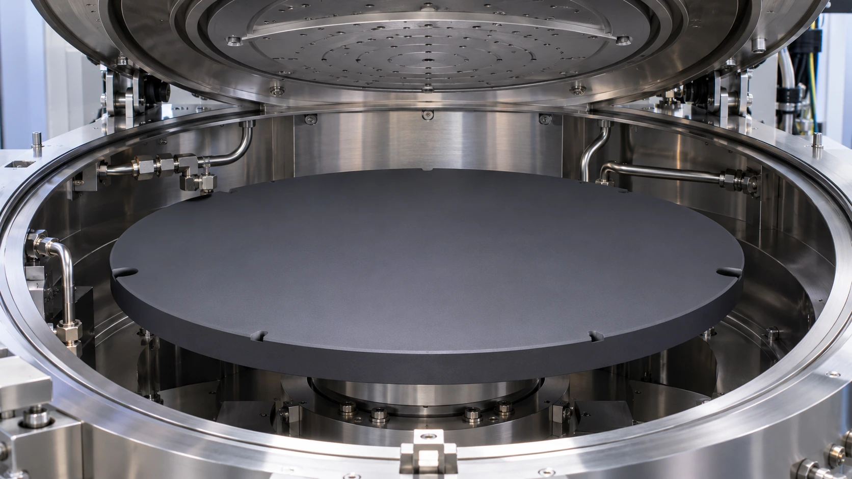
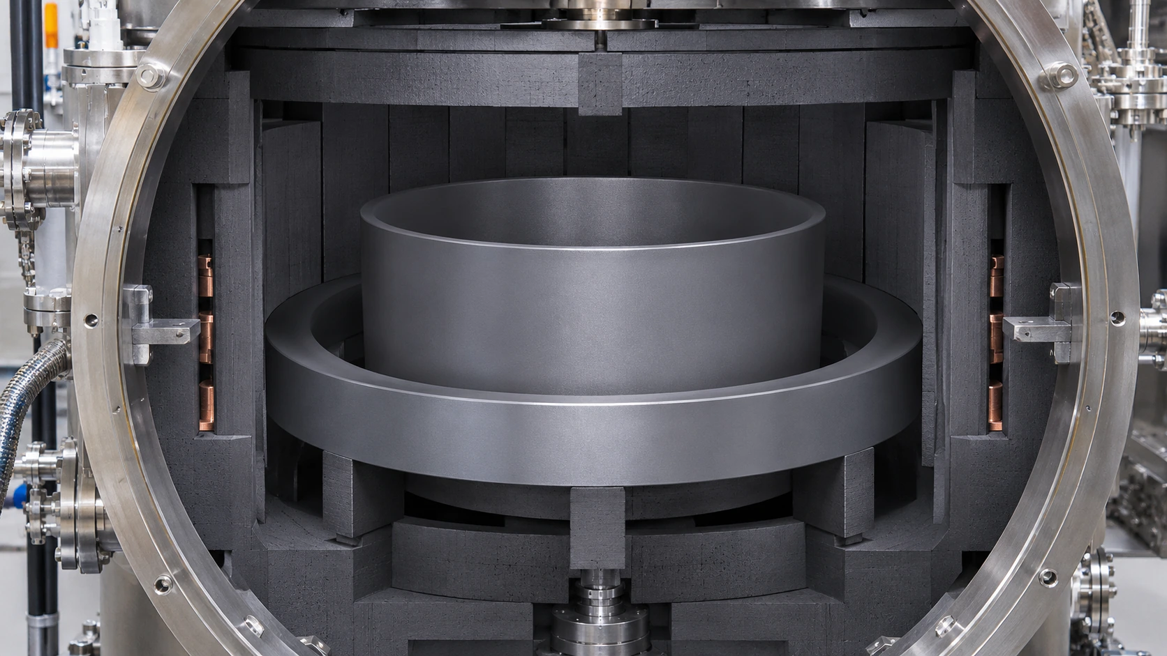
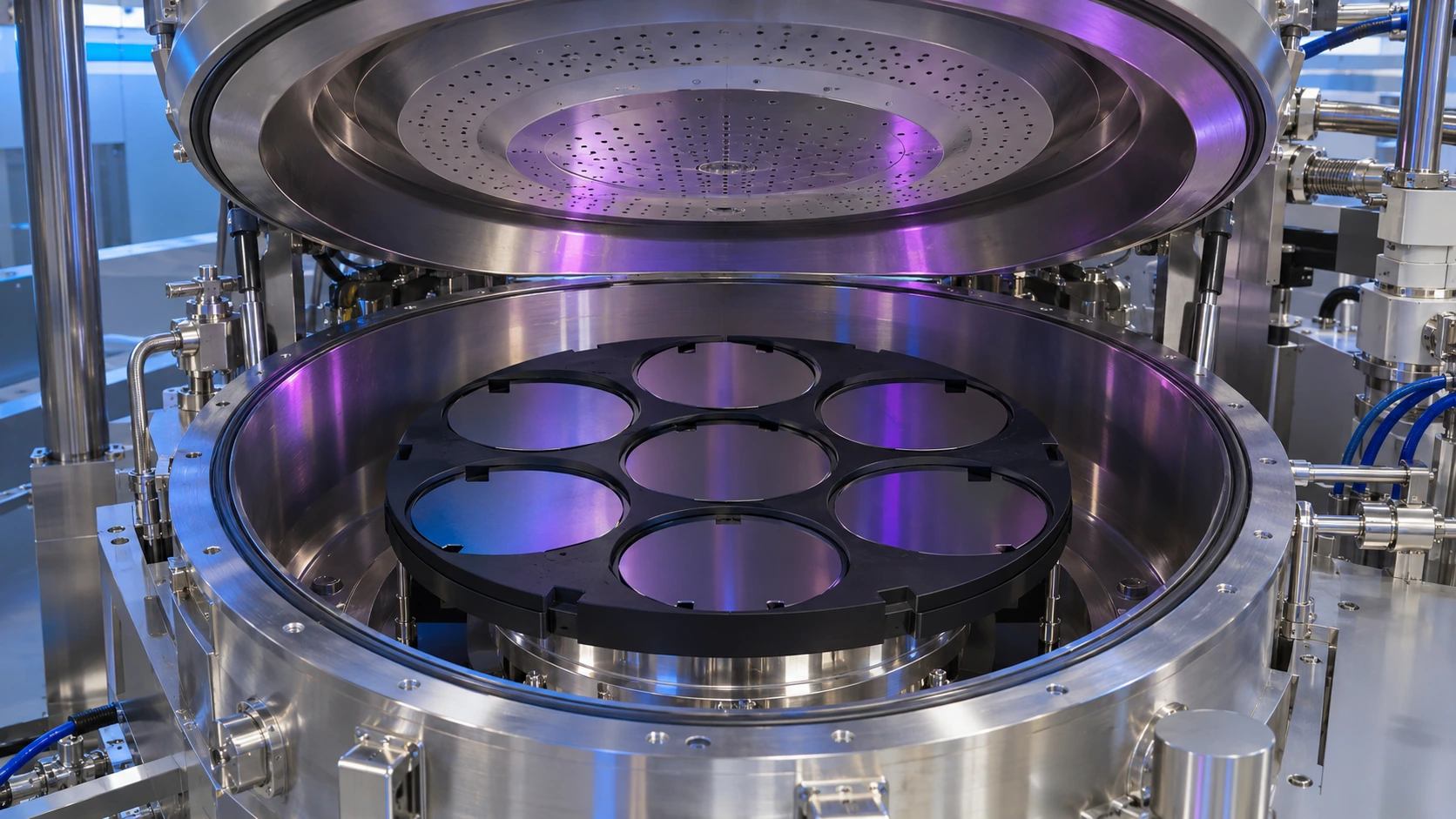
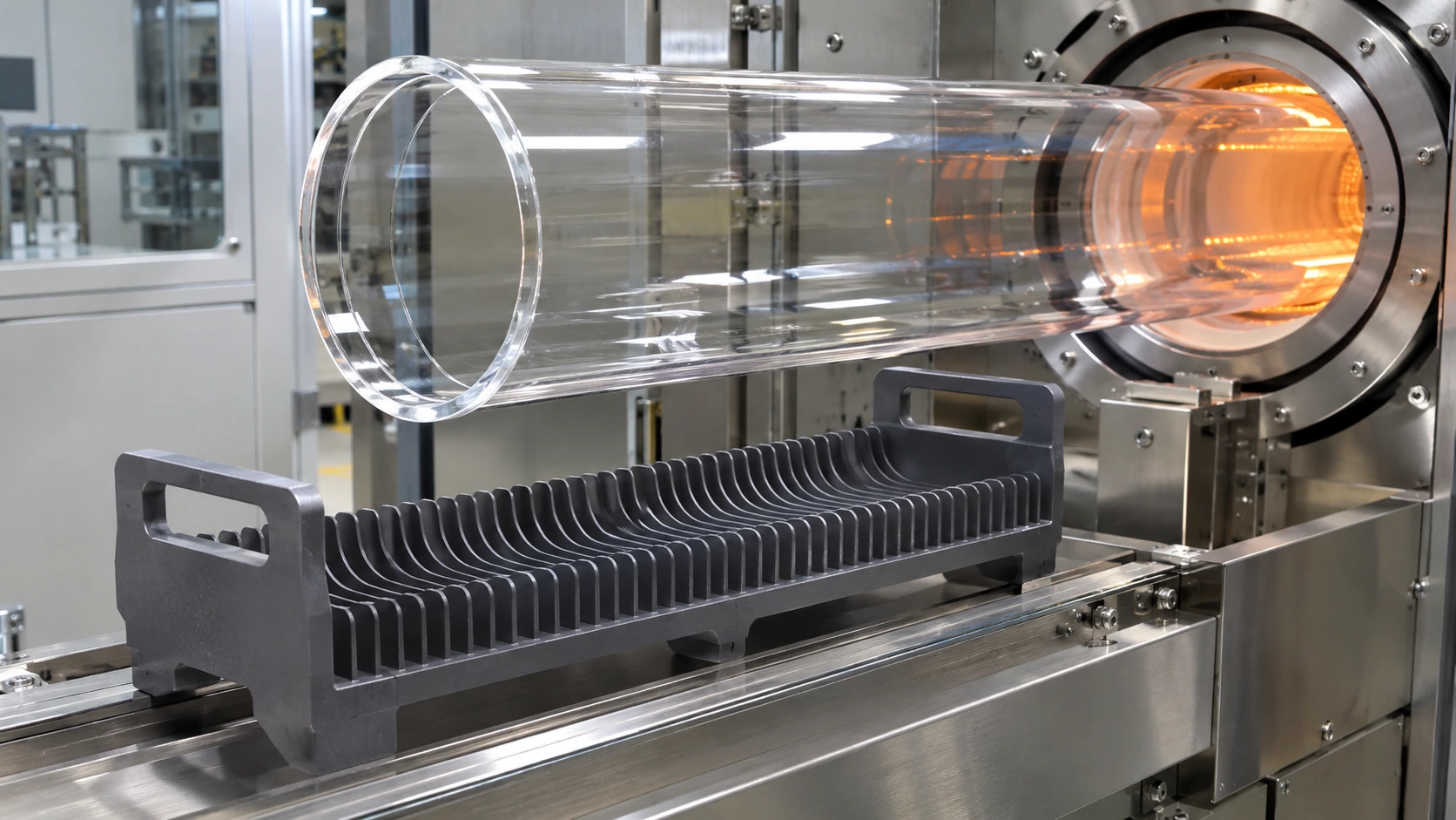
APPLICATION FIELDS.
Materials and components matched to the process chamber,from wafer deposition and crystal growth to high-temperature furnace steps.
TECHNICAL STRENGTHS.
Match materials, coatings and component geometry to the conditions inside your tool.
Material selection
Review operating temperature, atmosphere and surface requirements when choosing graphite, SiC or quartz.
CVD coatings
Define the surfaces that need SiC or TaC coverage, from wafer pockets to crystal growth fixtures.
Precision machining
Specify interfaces, tolerances and finishes around how the component locates and fits in the tool.
Inspection planning
Agree how critical dimensions and coating condition will be checked before production.
Selection guide
Start with your process temperature, chamber geometry, wafer size and required coating surfaces.
CUSTOM MANUFACTURING.
From drawing review and material selection to machining, coating and inspection, we develop parts around your process requirements.
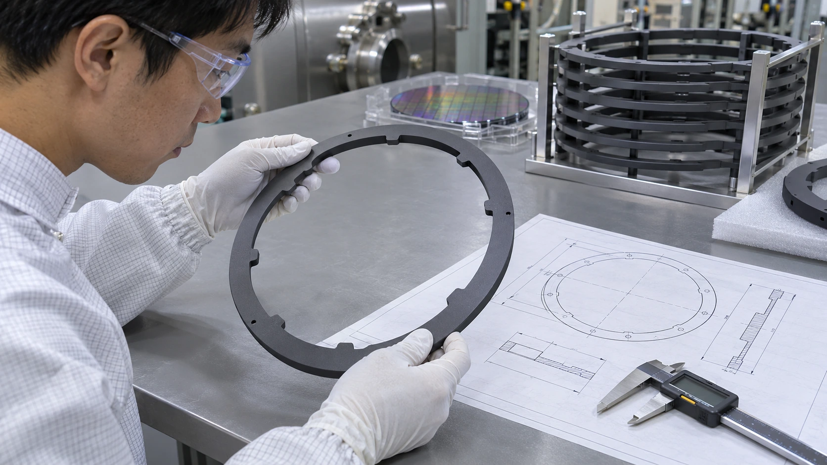
Start with the process.
Review drawings, operating conditions and the surfaces that matter to the process.
Discuss your requirements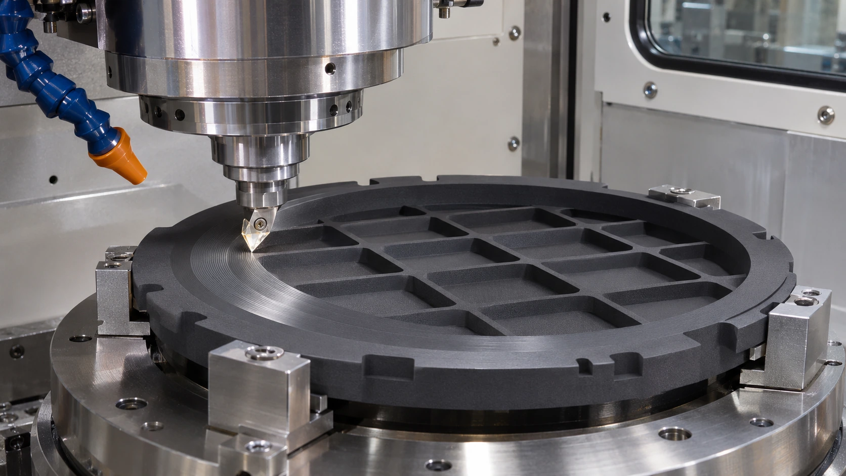
Machine and coat the part.
Translate the drawing into a component through precision machining and the specified coating process.
Discuss your requirements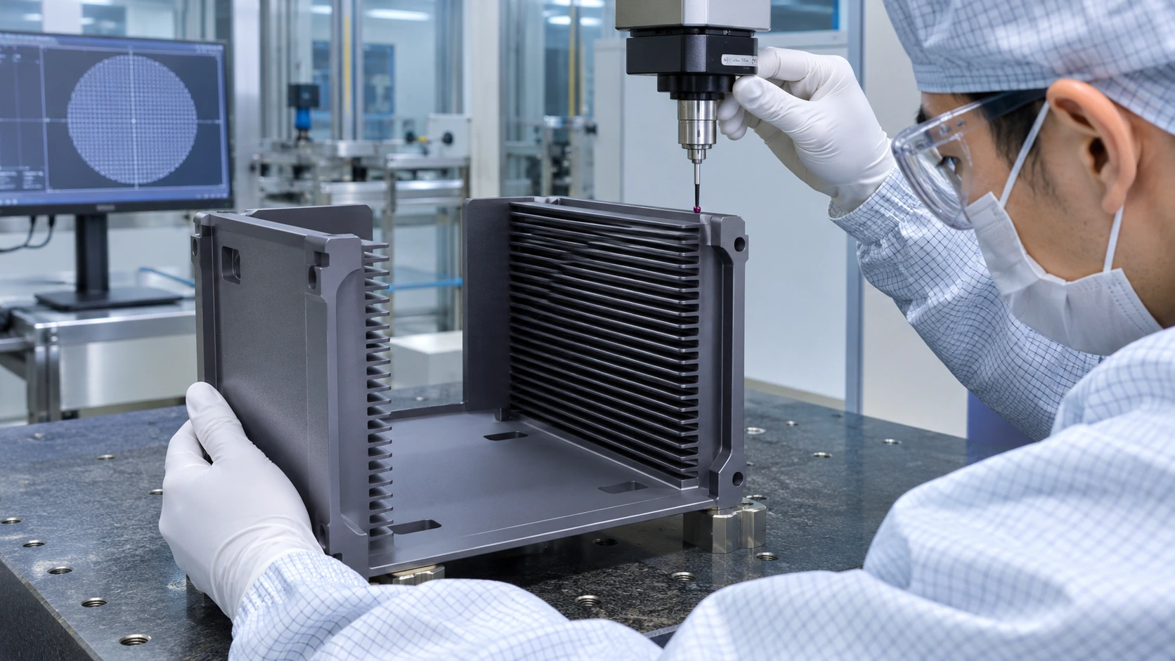
Verify the critical features.
Check dimensions and coating condition against the agreed inspection criteria.
Discuss your requirements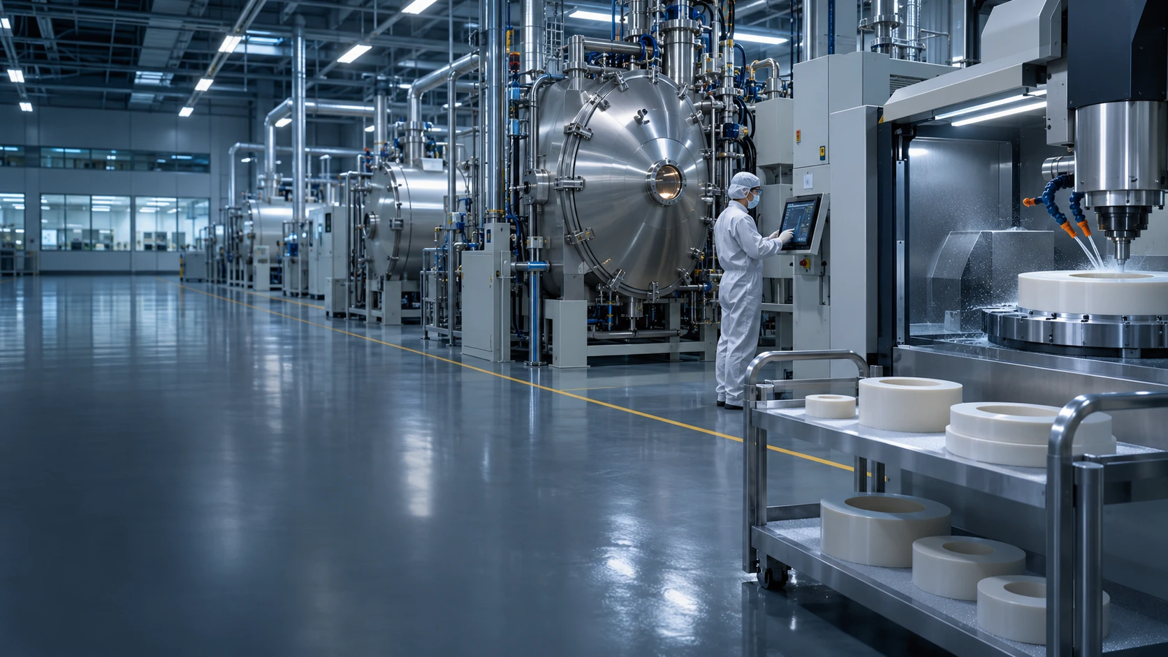
COMPANY
PROFILE.
Materials expertise.
Precision manufacturing.
Based in Ningbo, Semicera develops and manufactures materials and process components for semiconductor equipment.
Our work spans CVD coatings, precision machining and inspection for epitaxy, crystal growth and thermal processing.
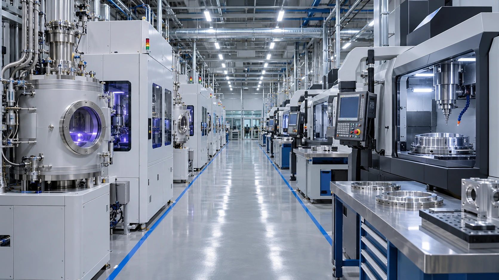
FACTORY & PRODUCTION.
Component machining, coating and inspection support the path from drawing to production.
QUALITY DOCUMENTATION.
Ask about the certification and inspection documents relevant to your component or supplier qualification.
PROJECT CASES.
Two engineering examples show how process conditions inform material and coating decisions.
Images are generated illustrations. These examples explain process considerations.
NEWS & INSIGHTS.
Browse insightsLET’S DISCUSS
YOUR COMPONENT.
Tell us about your process, operating conditions and the component you need.
sales01@semi-cera.com+86 133 7388 96831958 Jiangnan Road, Ningbo High-tech Zone,Zhejiang 315201, China
Tell us your application or the part you need in one sentence. We’ll use your contact details to respond to your inquiry.